1. Overview
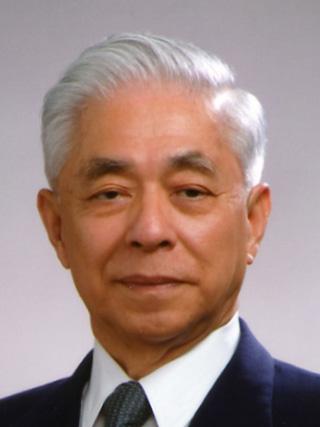
Jun-ichi Nishizawa (西澤 潤一Nishizawa Jun'ichiJapanese; September 12, 1926 - October 21, 2018) was a distinguished Japanese engineer and inventor, widely recognized as a pioneer whose foundational contributions significantly shaped the Information Age and the advancement of modern electronics. Often referred to as the "Father of Japanese Microelectronics" and "Mr. Semiconductor," Nishizawa made groundbreaking inventions in semiconductor devices, optical communication, and semiconductor process technologies. His notable inventions include the PIN diode, static induction transistor (SIT), and static induction thyristor (SITh), which laid the groundwork for technologies essential to the Internet and contemporary communication systems. He held an extensive portfolio of patents, reportedly the largest number of semiconductor-related patents globally, underscoring his prolific innovation. Beyond his scientific achievements, Nishizawa held prominent academic leadership roles, serving as President of Tohoku University and Iwate Prefectural University, and was a vocal advocate for originality in research and critical thinking. His lifelong dedication to pushing technological frontiers earned him numerous prestigious international and national awards, including the IEEE Edison Medal and the Order of Culture, and led to the establishment of the IEEE Jun-ichi Nishizawa Medal in his honor.
2. Biography
Jun-ichi Nishizawa's life was marked by a profound dedication to scientific inquiry and innovation, from his early education in Sendai to his influential career as a researcher and academic leader.
2.1. Early Life and Education
Jun-ichi Nishizawa was born on September 12, 1926, in Sendai, Miyagi Prefecture, Japan. He was the second child and eldest son of Kyosuke Nishizawa, a professor at Tohoku Imperial University. His younger brother, Taizo Nishizawa, also became a distinguished professor emeritus at Tohoku University, specializing in metallurgy. From a young age, Nishizawa displayed an inquisitive mind, famously questioning why "1 + 1 equals 2," demonstrating a fundamental skepticism and a deep desire to understand underlying principles.
He completed his early education at Katahira-cho Elementary School and Miyagi Prefectural Sendai Second Junior High School, graduating in March 1943. He then attended the Second Higher School (old system), graduating in March 1945. In April 1945, he was admitted to the Department of Electrical Engineering at Tohoku Imperial University's Faculty of Engineering based solely on his academic record. Although Nishizawa's personal ambition was to study nuclear physics or the foundations of mathematics in the Faculty of Science, his father, Kyosuke, did not permit it. His father, who remained influential in his life until his death at 103, consulted Heikichi Nukiyama, a professor in the Electrical Engineering department, who recommended Nishizawa join Yasushi Watanabe's laboratory. This decision proved pivotal, guiding Nishizawa into the nascent field of semiconductor solid-state devices. He earned his Bachelor of Science degree in 1948 and later a Doctor of Engineering degree in 1960, both from Tohoku University.
2.2. Early Career and Research
After graduating from the Faculty of Engineering, Nishizawa was accepted as a special graduate student, a system then in place. During this period, in 1950, he conceived his unique pin junction structure and invented semiconductor devices such as the PIN diode, static induction transistor, and pnip transistor. He also invented the crucial ion implantation method for semiconductor processing.
Despite his groundbreaking new theories, Nishizawa faced significant opposition from the academic community, which viewed his ideas as deviating from established norms. His mentor, Yasushi Watanabe, became concerned about this situation and, for a period, withheld Nishizawa's completed papers from external publication.
After completing his special graduate studies, Nishizawa was appointed as an assistant at the Research Institute of Electrical Communication at Tohoku University in April 1953. He continued his research and educational activities there until his mandatory retirement. In May 1954, he became an associate professor, and in December 1962, he was promoted to full professor. He served as the Director of the Research Institute of Electrical Communication from April 1983 to March 1986, and again from April 1989 to March 1990.
Building on the patent rights for his inventions like the PIN diode, Nishizawa, along with Watanabe and others, established the Semiconductor Research Promotion Foundation (1961-2008). This foundation, supported by donations from the industry, led to the establishment of the Semiconductor Research Institute in 1963, allowing Nishizawa to lead research initiatives outside the university setting. The foundation's assets were later donated to Tohoku University.
Nishizawa mentored and guided numerous students who went on to become prominent figures in their fields, including Fujio Masuoka, the inventor of flash memory; Masayoshi Esashi, a leading researcher in MEMS; Mitsumasa Koyanagi, known for his memory research; and Ikuo Nakamura, who developed marching memory. Among the faculty members in his laboratory was Tadahiro Ohmi, a distinguished researcher in semiconductor processes and cleanroom technology.
3. Major Inventions and Achievements
Jun-ichi Nishizawa's career was marked by a series of pioneering inventions that laid fundamental groundwork for modern electronics and communication.
3.1. Semiconductor Device Innovations
Nishizawa's work in semiconductor devices began in 1950 with his innovative theory of hot electron injection from a semiconductor to an insulator. Based on this theory, he conceived the pin structure, which involves an insulator (i) layer sandwiched within a pn junction. This led to the invention of several crucial devices:
- PIN diode**: Invented in 1950, this device is fundamental for high-frequency switching, attenuators, and photodiodes. The PIN photodiode was also invented by Nishizawa and his colleagues in 1950.

- Static induction transistor (SIT)**: Invented in 1950 with Y. Watanabe, the SIT is a high-speed, high-power device capable of operating at high temperatures.
- pnip transistor**: Also developed in 1950, this was an early transistor structure.
- Electron avalanche current amplification transistor**: Developed in 1951, this device utilized the avalanche phenomenon for current amplification.
- Avalanche photodiode (APD)**: Invented in 1952, APDs are highly sensitive photodetectors that use the avalanche effect to multiply the photocurrent.
- pnip drift transistor**: Developed in 1954.
- Transit-time negative resistance transistor**: Invented in 1954.
- Static induction thyristor (SITh)**: Invented in 1971, this device is a high-speed, high-power switching component used in power electronics.
- MOSSIT**: Proposed in 1971.
- Ideal SIT and Double-gate Static Induction Thyristor**: Further developments on his original concepts.
3.2. Optical Communication Technologies
Nishizawa made foundational contributions to optical communication, proposing key components that would later become essential for high-speed data transmission:
- Semiconductor optical maser**: In 1957, he proposed the concept of a semiconductor laser, a year before Arthur Leonard Schawlow and Charles H. Townes published their seminal paper on optical masers.
- Optical fiber communication**: In 1963, while at Tohoku University, he proposed the use of optical fibers for optical communication.
- Graded-index optical fiber (GI-type optical fiber)**: He invented and patented this in 1964. GI-type fibers enabled efficient light transmission over long distances by gradually changing the refractive index of the core, guiding light more effectively than step-index fibers.
- Photocoupler**: Invented in 1960.
- Optical thyristor (Optical Trigger Thyristor)**: Developed in 1984.
- Ultra-high-speed wideband optical modulator**: This technology was crucial for high-bandwidth optical data transmission.
3.3. Semiconductor Process Technologies
Nishizawa's innovations extended to the manufacturing processes of semiconductors, significantly improving device performance and crystal quality:
- Ion implantation**: Invented in 1950, this method precisely introduces impurities into semiconductors to alter their electrical properties.
- Stoichiometric composition control method**: Developed in 1951, essential for precise material composition.
- Electro-epitaxy**: Invented in 1954.
- Temperature difference method for silicon epitaxial growth**: Developed in 1963, this technique allowed for the growth of high-quality silicon layers.
- Vapor pressure liquid phase growth of gallium arsenide (GaAs)**: Developed in 1971.
- Vapor pressure controlled temperature difference liquid phase growth**: Invented in 1972.
- Stoichiometry controlled crystal growth method**: Developed in 1973.
- Photo-excited epitaxial growth**: Developed in 1984.
- Photo-excited molecular layer epitaxial growth (PMLE)**: Developed in 1984.
- GaAs perfect crystal growth method**: Focused on achieving highly pure and defect-free GaAs crystals.
- Ultra-thin metal molecular layer deposition and molecular layer epitaxial growth and doping of compound crystals**: These advanced techniques enabled the creation of extremely thin and precisely controlled semiconductor layers.
3.4. Other Inventions and Research
Nishizawa's research interests were broad, leading to other significant inventions and proposals:
- Solid-state maser**: Invented in 1955.
- Laser disc principle**: Proposed in 1957.
- Semiconductor inductance**: Invented in 1957.
- Varactor diode**: Invented in 1959.
- High-brightness LEDs**: He successfully developed high-brightness red (GaAlAs) and green (GaP) LEDs in 1976, overcoming the prevailing belief that bright LEDs were impossible.
- Terahertz wave generation**: In 1963, he proposed generating terahertz waves using molecular and lattice vibrations (phonons). His later work included THz Schottky diodes, semiconductor Raman lasers, and photo-excited processes for atomic layer etching of GaAs.
- Terahertz wave cancer diagnosis and treatment**: In 2000, he proposed using terahertz waves for the diagnosis and treatment of cancer.
- Millimeter wave multi-element oscillator using quasi-optical resonator**.
3.5. Patents and Intellectual Property
Jun-ichi Nishizawa was an exceptionally prolific inventor, holding over a thousand patents worldwide, a number that reportedly made him the individual with the world's largest number of semiconductor-related patents. His commitment to intellectual property was profound; he often drafted his patent applications himself rather than relying solely on patent attorneys.
However, his journey with patents was not without significant challenges. For instance, his patent application for optical fiber faced initial rejection due to procedural deficiencies, leading to a prolonged legal battle with the Japan Patent Office and opposition from other parties. This lengthy dispute ultimately resulted in the patent's expiration before its full commercial potential could be realized.
Nishizawa also expressed strong dissatisfaction with how Japanese industries often undervalued and underutilized the inventions of domestic researchers. He recounted an experience with his PIN diode patent: despite having secured the patent in Japan before General Electric (GE) obtained a similar one in the United States, Japanese companies frequently paid royalties to GE without properly investigating or acknowledging Nishizawa's earlier, valid patent in Japan. Even after his patent's validity became widely known in Japan, he received minimal royalties from Japanese firms. He noted that while the Semiconductor Research Promotion Foundation was established with approximately 70.00 M JPY in investments based on his patents, this amount was significantly "discounted" compared to what Japanese companies were paying GE. Nishizawa critically observed that the issue was not a lack of originality among Japanese inventors, but rather the domestic industry's failure to properly evaluate and industrialize the achievements of its own people.
3.5.1. List of US Patents
| Patent Number |
|---|
| US3896484 |
| US4465527 |
| US4526632 |
| US4613881 |
| US4619718 |
| US4685979 |
| US4720735 |
| US4772926 |
| US4819058 |
| US4841350 |
| US4872044 |
| US4935798 |
| US5001535 |
| US5357361 |
4. Academic and Professional Career
Nishizawa's career extended beyond invention into significant academic and leadership roles, where he shaped future generations of engineers and influenced university administration.
4.1. Professorship and Research Activities
After joining the Research Institute of Electrical Communication at Tohoku University as an assistant in April 1953, Nishizawa steadily advanced through the academic ranks, becoming an associate professor in May 1954 and a full professor in December 1962. During his tenure, he dedicated himself to both groundbreaking research and the mentorship of numerous students. He served two terms as Director of the Research Institute of Electrical Communication, from April 1983 to March 1986 and again from April 1989 to March 1990. His guidance produced many notable scholars and inventors, including Fujio Masuoka, who invented flash memory, and Masayoshi Esashi, a prominent researcher in MEMS.
4.2. University Leadership Roles
In April 1990, Nishizawa was appointed Professor Emeritus at Tohoku University. Later that year, in November 1990, he assumed the prestigious role of President of Tohoku University, a position he held until March 1996, following the death in office of his predecessor, Shigemori Otani. After his tenure at Tohoku University, he continued to contribute to higher education in significant leadership capacities:
- President of Iwate Prefectural University**: From April 1998 to March 2005, becoming its first president and later an honorary president in August 2005.
- President of Tokyo Metropolitan University**: From April 2005 to March 2009.
- Special Professor at Sophia University**: From August 2005.
- Honorary President of Miyagi University**: From September 1997.
4.3. Research Promotion and Industry Engagement
Nishizawa was deeply committed to fostering research and development beyond traditional academic settings. In May 1968, he became the Director of the Semiconductor Research Institute, a part of the Semiconductor Research Promotion Foundation. This foundation, established in 1961 based on the patent rights of Nishizawa and his colleagues, aimed to promote semiconductor research with industrial support. He also served as the Chairman of the Tohoku University Electrical Engineering Alumni Association from 1999 to 2004.
He held numerous other external positions, demonstrating his broad engagement with scientific, industrial, and public organizations. These included roles such as Chairman of the Advanced Technology Industry Strategy Promotion Organization, Director of the Matsumae International Foundation, Advisor to the Japan Heat Island Institute, and Advisor to the Science and Technology Exchange Foundation. He also served as President of the Atomic Fuel Policy Research Council and Chairman of the ITSS User Association.
5. Philosophy and Vision
Jun-ichi Nishizawa's approach to science and technology was deeply rooted in a philosophy that championed originality and challenged conventional wisdom.
5.1. Originality and Innovation Theory
Nishizawa was a staunch advocate for "originality" (独創DokusoJapanese). He believed that true innovation meant pioneering new frontiers rather than merely following existing paths. He famously stated that "to achieve originality, one must be a heretic," emphasizing the importance of independent thought, even if it meant challenging established academic and industrial norms. This philosophy was shaped by his own experiences, such as his initial failure to replicate a solid-state amplifier experiment using iron pyrite, which was documented in early literature, and his successful development of high-brightness red LEDs despite the prevailing belief that such an achievement was impossible. His proposal for optical communication through glass (a dielectric) also met with strong criticism from academic authorities, further solidifying his belief in the necessity of a skeptical and unconventional approach to research.
5.2. Technological Development Perspectives
Nishizawa held strong views on the direction of technological progress and the role of industry in adopting new innovations. He was critical of what he perceived as a tendency within Japanese industry to undervalue and underutilize the achievements of domestic researchers. He pointed to his own experiences with patents, where Japanese companies often paid royalties to foreign entities for technologies that he had already patented in Japan, or largely ignored his groundbreaking work. He argued that the problem was not a lack of originality among Japanese inventors, but rather a systemic issue within Japan where the achievements of compatriots were neither properly evaluated nor industrialized.
He also possessed a remarkable foresight regarding the global semiconductor industry. In 1990, he predicted that the leadership in the semiconductor industry would shift from Japan to South Korea, then to China, and eventually to Vietnam. This "prophecy," as noted by the Chosun Ilbo in 2018, proved largely accurate, highlighting his deep understanding of global technological and economic dynamics. He had cultivated relationships with figures like Lee Byung-chul, the founder of Samsung Group, who frequently visited Nishizawa at Tohoku University in the mid-1970s to seek his guidance on semiconductor technology.
6. Personal Life and Family
Beyond his scientific and professional endeavors, Jun-ichi Nishizawa's personal life was rich with diverse interests and a notable family background.
6.1. Family Background
Nishizawa's family tree reveals a lineage connected to prominent figures in academia and business. His paternal grandfather was Chozaburo Takemoto VII, the founder of Takemoto Oil & Fat Co., Ltd.. His paternal adoptive grandfather, Kinjiro Nishizawa, was a landlord in Ushigome, Tokyo. Kinjiro, originally from a poor samurai family named Abe, rose from an apprentice to a head clerk at the pharmaceutical company Omura Shiseido before becoming a successful landlord. He adopted the Nishizawa surname by purchasing the family register of the former Kanazawa domain's Nishizawa family. Jun-ichi's maternal grandmother, Yae, was also a daughter of Omura Shiseido, being the younger sister of Kinjiro's wife. Omura Shiseido was a branch of the original Shiseido company during the Meiji period.
His father, Kyosuke Nishizawa (1892-1995), was the second son of Chozaburo Takemoto VII but was adopted into the Nishizawa family after graduating from the old-system Eighth Higher School. Kyosuke graduated from the Department of Applied Chemistry at Kyushu Imperial University's Faculty of Engineering, becoming the university's first Doctor of Engineering in 1922. He later became an assistant professor (and later professor) at Tohoku Imperial University, where he conducted pioneering research on fat-decomposing agents and sulfated oils. In 1935, he provided technical guidance for the manufacture of surfactants at his family's company, Takemoto Oil & Fat. He served as the 10th Dean of the Faculty of Engineering and retired in 1955, passing away at the age of 103.
Jun-ichi's younger brother was Taizo Nishizawa, a distinguished metallurgist and professor emeritus at Tohoku University. His wife, Takeko, was the second daughter of Tanezō Hayakawa. His daughter, Keiko Takahashi, is married to diplomat Koichi Takahashi. Jun-ichi had originally wanted to name his daughter "Keiko" (珪子), using the kanji for silicon (珪), to reflect the shift in semiconductor materials from germanium to silicon, but this was not possible due to restrictions on kanji usage at the time. Keiko Takahashi authored the book Mr. Semiconductor Jun-ichi Nishizawa as a Father: Seeking Light and Beyond in 2024. His second cousin was Isao Tomita, the renowned composer, arranger, and synthesizer musician.
6.2. Hobbies and Interests
Nishizawa had a lifelong passion for art. From his elementary school days, he enjoyed painting and joined the art club in junior high school. Later in life, 121 watercolors and pen drawings created between the ages of 14 and 24 were discovered. However, his intense dedication to research prevented him from pursuing painting further.
He was also a great admirer of the French Impressionist painter Claude Monet. In 1971, during a visit to the Musée Marmottan Monet in Paris, he noticed that a painting from Monet's Water Lilies series, which depicted the sky reflected on the water's surface, was displayed upside down. He pointed this out, and when it remained uncorrected the following year, he again brought it to attention, leading to the incident being reported in the French newspaper Le Monde.
Another of his hobbies was 8mm filmmaking. He began filming in his youth, and some of his early films, including footage of his laboratory from around 1955, are preserved as valuable historical records of his research environment.
7. Awards and Honors
Jun-ichi Nishizawa received extensive recognition for his profound contributions to science and engineering, both domestically and internationally.
7.1. Major Scientific and Engineering Awards
Nishizawa was honored with numerous prestigious awards for his groundbreaking inventions and research:
- Science and Technology Agency Director-General's Commendation** (October 1965) for "Impurity Inhomogeneous Semiconductor."
- Imperial Invention Prize** (April 1966) for "Impurity Inhomogeneous Semiconductor."
- Matsunaga Prize** (December 1969) for "Research on Semiconductor Devices."
- Science and Technology Agency Director-General's Commendation** (November 1970) for "Semiconductor Maser."
- Okouchi Memorial Technology Prize** (April 1971) for "Development of Silicon Varactor Diode by Alloy Diffusion Method."
- Japan Academy Prize** (June 1974) for "Research on Semiconductors and Transistors."
- Science and Technology Achievement Award** (April 1975) for "Development of Static Induction Field Effect Transistor."
- Institute of Electronics and Communication Engineers of Japan Achievement Award** (May 1975) for "High-Performance Transistor with New Triode Characteristics."
- Tohoku Regional Invention Award, Miyagi Prefecture Branch Director's Prize** (October 1975) for "Position Control Device."
- Okouchi Memorial Technology Prize** (March 1980) for "Development of Continuous Growth Technology for High-Brightness Light-Emitting Diodes."
- Japan Patent Office Commissioner's Commendation** (October 1980) for "Manufacturing Method and Apparatus for Semiconductor Devices by Continuous Liquid Phase Growth."
- Inoue Harushige Award** (July 1982) for "Continuous Manufacturing Technology of High-Brightness Light-Emitting Diodes."
- IEEE Jack A. Morton Award** (December 1983) for "Development of SIT (Static Induction Transistor) and the three basic elements of optical communication."
- Asahi Prize** (1984) for "Research on Optical Communication and Semiconductors."
- Honda Prize** (1986) for "inventing the PIN diode, static induction transistor, and contributing to the application and development of optical communication technology."
- Laudise Prize of the International Organization for Crystal Growth (IOCG)** (1989).
- Okawa Prize** (1996) for "original research in materials science, development of semiconductor engineering, and pioneering achievements and significant contributions to optical communication."
- IEEE Edison Medal** (2000).
7.2. National and International Recognition
Nishizawa's contributions were recognized with high national honors and international accolades:
- Medal with Purple Ribbon** (October 1975) for "Perfect Crystals and Static Induction Transistors."
- Person of Cultural Merit** (November 1983) for his work in semiconductor engineering.
- Order of Culture** (November 1989) for his achievements in electronic engineering.
- Honorary Citizen of Miyagi Prefecture** (1990).
- Grand Cordon of the Order of the Sacred Treasure** (2002).
- IEEE** recognized him as "one of the geniuses of the 20th century" in a statement accompanying the establishment of the Nishizawa Medal. He was a Life Fellow of the IEEE and a Fellow of several other institutions, including the Physical Society of Japan, the Russian Academy of Sciences, and the Polish Academy of Sciences.
8. Impact and Legacy
Jun-ichi Nishizawa's work had a profound and lasting impact on the fields of science, technology, and industry, shaping the modern world.
8.1. Influence on Science and Technology
Nishizawa's inventions fundamentally advanced microelectronics and laid crucial groundwork for the Information Age. His development of the PIN diode, static induction transistor, and static induction thyristor provided essential components for high-speed, high-power electronic devices that are ubiquitous today. His pioneering proposals for semiconductor lasers and optical fiber communication were visionary, preceding much of the globally recognized work in these fields. While Charles K. Kao later received the Nobel Prize in Physics in 2009 for his work on optical fibers, Nishizawa's contributions to the underlying principles and components, such as the graded-index optical fiber, were instrumental in making fiber optic communication a reality. His innovations in semiconductor process technologies, including ion implantation and various epitaxial growth methods, significantly improved the quality and performance of semiconductor crystals, enabling the miniaturization and efficiency of integrated circuits.
8.2. Societal and Industrial Contributions
The practical impact of Nishizawa's technologies on modern communication and information access is immense. His work directly contributed to the development of the Internet and the infrastructure that supports global digital communication. The high-brightness LEDs he developed are now common in displays, lighting, and various electronic devices.
Beyond his direct inventions, Nishizawa's influence extended to industrial strategy. His prophetic observations in 1990 about the shift in global semiconductor industry leadership from Japan to South Korea, then China, and eventually Vietnam, demonstrated a keen understanding of geopolitical and technological trends. This foresight, partly informed by his interactions with figures like Lee Byung-chul of Samsung, underscored his broader impact on the strategic thinking within the technology sector.
8.3. Critical Perspectives and Evaluations
Despite his monumental achievements, Nishizawa faced significant challenges in gaining full recognition and adoption of his innovations within his home country. He often expressed frustration with what he perceived as a lack of appreciation for domestic research and a tendency for Japanese companies to overlook or undervalue the work of Japanese scientists. His experiences with patent disputes, particularly regarding his PIN diode patent where Japanese firms paid royalties to foreign companies despite his earlier domestic patent, highlighted a systemic issue he believed hindered Japan's technological advancement. He argued that the problem was not a lack of originality among Japanese inventors, but rather the failure of Japanese industry to properly evaluate and industrialize the achievements of its own people. This critical perspective, born from his personal struggles for recognition, adds a nuanced layer to his legacy, emphasizing the complex interplay between scientific innovation, industrial adoption, and national strategy.
9. Commemoration
To honor his immense contributions, several initiatives and institutions have been established in Jun-ichi Nishizawa's memory.
9.1. IEEE Jun-ichi Nishizawa Medal
In 2002, the Institute of Electrical and Electronics Engineers (IEEE) established the IEEE Jun-ichi Nishizawa Medal. This prestigious medal, supported by the Federation of Electric Power Companies, is awarded to individuals or groups who have made outstanding contributions in the fields of electronic devices and materials science. The creation of this medal serves as a lasting tribute to Nishizawa's pioneering spirit and his profound impact on the global microelectronics industry, recognizing him as one of the true geniuses of the 20th century.
10. Further Information
10.1. Notable Publications
Jun-ichi Nishizawa authored several books, sharing his insights on technology, innovation, education, and societal challenges:
- Fighting Original Technology (日刊工業新聞社, 1981)
- Foolish and Resolute - My Resume (日本経済新聞社, 1985)
- Originality Lies in Struggle (プレジデント社, 1986; 新潮社, 1989)
- Jun-ichi Nishizawa's Theory of Original Development (工業調査会, 1986)
- Reading the Future of 'Technology Superpower Japan' (PHP研究所, 1989)
- My Romance and Science (中央公論社, 1990)
- Original Education Will Save Japan (PHP研究所, 1991)
- Humanity is Heading Towards Extinction (潮出版社, 1993)
- The Era of Tohoku - No Longer a Unipolar Concentration (潮出版社, 1995)
- Rethinking the Purpose of Education (岩波書店, 1996)
- New Recommendations for Learning - How to Live in the 21st Century (本の森, 1997)
- Stand Tall, Japanese People (PHP研究所, 1999)
- Humanity Will Perish in 80 Years (東洋経済新報社, 2000)
- Saving the Education-Destroyed Nation (本の森, 2000)
- Discovery of Red, Discovery of Blue (白日社, 2001)
- Japanese People, Have Romance (本の森, 2002)
- Strategic Original Development (工業調査会, 2006)
- The Power to Create (PHP研究所, 2010)
- If I Were to Talk About Exploration (ポプラ社, 2010)
10.2. External Links
- [http://www.ieeeghn.org/wiki/index.php/Jun-ichi_Nishizawa Jun-ichi Nishizawa - Biographical article on IEEE Global History Network]